- 您现在的位置:买卖IC网 > Sheet目录3832 > PIC18F2520-I/ML (Microchip Technology)IC PIC MCU FLASH 16KX16 28QFN
PIC16(L)F1782/3
DS41579C-page 324
Preliminary
2011-2012 Microchip Technology Inc.
27.1.2.8
Asynchronous Reception Set-up:
1.
Initialize the SPBRGH, SPBRGL register pair
and the BRGH and BRG16 bits to achieve the
desired baud rate (see Section 27.4 “EUSART
2.
Clear the ANSEL bit for the RX pin (if applicable).
3.
Enable the serial port by setting the SPEN bit.
The SYNC bit must be clear for asynchronous
operation.
4.
If interrupts are desired, set the RCIE bit of the
PIE1 register and the GIE and PEIE bits of the
INTCON register.
5.
If 9-bit reception is desired, set the RX9 bit.
6.
Enable reception by setting the CREN bit.
7.
The RCIF interrupt flag bit will be set when a
character is transferred from the RSR to the
receive buffer. An interrupt will be generated if
the RCIE interrupt enable bit was also set.
8.
Read the RCSTA register to get the error flags
and, if 9-bit data reception is enabled, the ninth
data bit.
9.
Get the received 8 Least Significant data bits
from the receive buffer by reading the RCREG
register.
10. If an overrun occurred, clear the OERR flag by
clearing the CREN receiver enable bit.
27.1.2.9
9-bit Address Detection Mode Set-up
This mode would typically be used in RS-485 systems.
To set up an Asynchronous Reception with Address
Detect Enable:
1.
Initialize the SPBRGH, SPBRGL register pair
and the BRGH and BRG16 bits to achieve the
desired baud rate (see Section 27.4 “EUSART
2.
Clear the ANSEL bit for the RX pin (if applicable).
3.
Enable the serial port by setting the SPEN bit.
The SYNC bit must be clear for asynchronous
operation.
4.
If interrupts are desired, set the RCIE bit of the
PIE1 register and the GIE and PEIE bits of the
INTCON register.
5.
Enable 9-bit reception by setting the RX9 bit.
6.
Enable address detection by setting the ADDEN
bit.
7.
Enable reception by setting the CREN bit.
8.
The RCIF interrupt flag bit will be set when a
character with the ninth bit set is transferred
from the RSR to the receive buffer. An interrupt
will be generated if the RCIE interrupt enable bit
was also set.
9.
Read the RCSTA register to get the error flags.
The ninth data bit will always be set.
10. Get the received 8 Least Significant data bits
from the receive buffer by reading the RCREG
register. Software determines if this is the
device’s address.
11. If an overrun occurred, clear the OERR flag by
clearing the CREN receiver enable bit.
12. If the device has been addressed, clear the
ADDEN bit to allow all received data into the
receive buffer and generate interrupts.
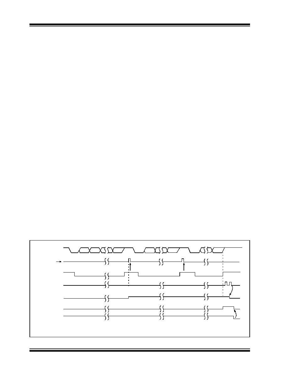
FIGURE 27-5:
ASYNCHRONOUS RECEPTION
Start
bit
bit 7/8
bit 1
bit 0
bit 7/8
bit 0
Stop
bit
Start
bit
Start
bit
bit 7/8 Stop
bit
RX/DT pin
Reg
Rcv Buffer Reg.
Rcv Shift
Read Rcv
Buffer Reg.
RCREG
RCIF
(Interrupt Flag)
OERR bit
CREN
Word 1
RCREG
Word 2
RCREG
Stop
bit
Note:
This timing diagram shows three words appearing on the RX input. The RCREG (receive buffer) is read after the third word,
causing the OERR (overrun) bit to be set.
RCIDL
发布紧急采购,3分钟左右您将得到回复。
相关PDF资料
AT87C51RC2-SLSUL
IC 8051 MCU 32K OTP 30MHZ 44PLCC
AT87C51RC2-RLTUM
IC 8051 MCU 32K OTP 40MHZ 44VQFP
AT87C51RC2-RLTUL
IC 8051 MCU 32K OTP 30MHZ 44VQFP
213684-4
34 PLUG KIT,M-SER,CC,JS,W/HOOD
202515-3
CONN PLUG BLOCK 42POS BLUE
202515-2
CONN PLUG M-SERIES 42POS
AT87C51RB2-RLTUL
IC 8051 MCU 16K OTP 30MHZ 44VQFP
AT87C51RB2-3CSUM
IC 8051 MCU 16K OTP 40MHZ 40DIP
相关代理商/技术参数
PIC18F2520-I/ML
制造商:Microchip Technology Inc 功能描述:8-Bit Microcontroller IC
PIC18F2520-I/SO
功能描述:8位微控制器 -MCU 32KB 1536 RAM 25I/0 RoHS:否 制造商:Silicon Labs 核心:8051 处理器系列:C8051F39x 数据总线宽度:8 bit 最大时钟频率:50 MHz 程序存储器大小:16 KB 数据 RAM 大小:1 KB 片上 ADC:Yes 工作电源电压:1.8 V to 3.6 V 工作温度范围:- 40 C to + 105 C 封装 / 箱体:QFN-20 安装风格:SMD/SMT
PIC18F2520-I/SP
功能描述:8位微控制器 -MCU 32KB 3968 RAM 25I/O RoHS:否 制造商:Silicon Labs 核心:8051 处理器系列:C8051F39x 数据总线宽度:8 bit 最大时钟频率:50 MHz 程序存储器大小:16 KB 数据 RAM 大小:1 KB 片上 ADC:Yes 工作电源电压:1.8 V to 3.6 V 工作温度范围:- 40 C to + 105 C 封装 / 箱体:QFN-20 安装风格:SMD/SMT
PIC18F2520T-E/SO
功能描述:8位微控制器 -MCU 32KB Flash 1536RAM 23I/O RoHS:否 制造商:Silicon Labs 核心:8051 处理器系列:C8051F39x 数据总线宽度:8 bit 最大时钟频率:50 MHz 程序存储器大小:16 KB 数据 RAM 大小:1 KB 片上 ADC:Yes 工作电源电压:1.8 V to 3.6 V 工作温度范围:- 40 C to + 105 C 封装 / 箱体:QFN-20 安装风格:SMD/SMT
PIC18F2520T-I/ML
功能描述:8位微控制器 -MCU 32KB 3968 RAM 25I/O RoHS:否 制造商:Silicon Labs 核心:8051 处理器系列:C8051F39x 数据总线宽度:8 bit 最大时钟频率:50 MHz 程序存储器大小:16 KB 数据 RAM 大小:1 KB 片上 ADC:Yes 工作电源电压:1.8 V to 3.6 V 工作温度范围:- 40 C to + 105 C 封装 / 箱体:QFN-20 安装风格:SMD/SMT
PIC18F2520T-I/SO
功能描述:8位微控制器 -MCU 32KB 3968 RAM 25I/O RoHS:否 制造商:Silicon Labs 核心:8051 处理器系列:C8051F39x 数据总线宽度:8 bit 最大时钟频率:50 MHz 程序存储器大小:16 KB 数据 RAM 大小:1 KB 片上 ADC:Yes 工作电源电压:1.8 V to 3.6 V 工作温度范围:- 40 C to + 105 C 封装 / 箱体:QFN-20 安装风格:SMD/SMT
PIC18F2523-E/ML
功能描述:8位微控制器 -MCU 32KB FL 1536bytes- RAM 25I/O RoHS:否 制造商:Silicon Labs 核心:8051 处理器系列:C8051F39x 数据总线宽度:8 bit 最大时钟频率:50 MHz 程序存储器大小:16 KB 数据 RAM 大小:1 KB 片上 ADC:Yes 工作电源电压:1.8 V to 3.6 V 工作温度范围:- 40 C to + 105 C 封装 / 箱体:QFN-20 安装风格:SMD/SMT
PIC18F2523-E/SO
功能描述:8位微控制器 -MCU 32KB FL 1536bytes- RAM 25I/O RoHS:否 制造商:Silicon Labs 核心:8051 处理器系列:C8051F39x 数据总线宽度:8 bit 最大时钟频率:50 MHz 程序存储器大小:16 KB 数据 RAM 大小:1 KB 片上 ADC:Yes 工作电源电压:1.8 V to 3.6 V 工作温度范围:- 40 C to + 105 C 封装 / 箱体:QFN-20 安装风格:SMD/SMT